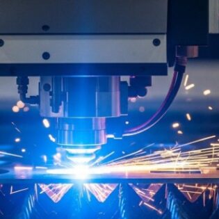
In the PCB manufacturing industry, thick copper boards have become the core substrate for power modules, high-power electronic devices, and industrial control systems due to their exceptional conductivity and thermal dissipation properties. As copper thickness increases from the conventional 1-3 ounces to 6 ounces or even higher, their processing technology faces unprecedented challenges.
Drilling, as a critical process in PCB production, presents unique physical phenomena and process contradictions when working with thick copper boards:
The high thermal conductivity significantly reduces cutting temperatures
The plastic deformation characteristics of copper cause secondary issues like copper wrapping and material adhesion
Behind these contradictions lies a complex interplay of materials science, mechanical processing, and thermodynamics.
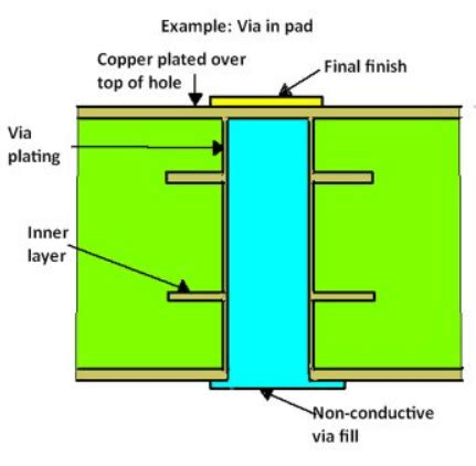
The Thermodynamic Paradox in Thick Copper PCB Drilling
With a thermal conductivity of 401 W/(m·K) – approximately 1.8 times that of aluminum and 5 times that of iron – copper exhibits unique thermal behavior during drilling operations. The rapid heat dissipation through the copper substrate theoretically suppresses temperature rise between tool and workpiece, yielding dual benefits:
? Tool wear rate reduction by ~30%
? Over 50% decrease in positional accuracy deviation caused by thermal deformation
These characteristics make it particularly suitable for high-precision multilayer board processing.
However, this seemingly ideal thermal property conceals a paradox:
During initial drill penetration, copper’s instantaneous plastic flow creates a high-pressure zone ahead of the cutting edge. While bulk temperatures remain low, frictional heat at microscopic contact points can momentarily reach copper’s recrystallization temperature (~200°C).

This phenomenon causes dynamic softening of the copper surface layer, forming a viscous metal flow. When drill speed exceeds 80,000 RPM, the contact time between chips and the tool’s rake face shortens to microsecond levels. However, the ductility of copper chips makes them difficult to break effectively, instead forming long spiral chips under centrifugal force. These copper wires entangle between the drill shank and chip flutes, not only hindering coolant penetration but also generating secondary frictional heat. Experimental data shows that when copper thickness exceeds 4 ounces, the localized temperature rise caused by chip entanglement can reach 40% of the base cutting temperature, creating a “l(fā)ow-temperature cutting with localized high-temperature” paradox effect.
Plastic Behavior of Materials and Generation Mechanism of Machining Defects
Pure copper has an elongation rate as high as 45%, and this excellent plasticity manifests as three-stage deformation characteristics during drilling: lattice slip during initial shear, dislocation multiplication during plastic flow, and necking before fracture. When drilling thick copper boards, increased axial cutting depth makes the material removal process closer to an orthogonal cutting model, reducing the shear plane angle to 15°-25° and increasing chip thickness by 30%-50%. These thick, continuous chips intermittently contact the hole wall during ejection, forming a periodic stick-slip dynamic process.
The essence of copper adhesion is interfacial metallurgical bonding. When cutting temperature reaches copper’s recrystallization temperature, fresh copper surfaces undergo atomic diffusion with the tool surface under high pressure. Even with relatively low bulk temperatures, instantaneous temperatures at microscopic asperities can exceed 500°C, sufficient to cause micro-welding. When using tungsten carbide drills, cobalt binder phase precipitation accelerates this adhesion. EDX analysis shows adhesion layers can contain up to 8.3wt% cobalt, forming Co-Cu intermetallic compounds. These metallurgical bonding layers have shear strength up to 350MPa – three times copper’s own strength – causing negative offset of the tool’s effective rake angle and increasing cutting force by over 25%.
Coordinated Optimization of Process Parameters and Tool Design
Addressing thick copper board drilling challenges requires establishing a multi-dimensional process control system. For cutting parameters, the “high speed-low feed” strategy presents contradictions: increasing speed to 90,000 RPM can reduce feed per tooth to 0.01mm, helping thin chips, but greater centrifugal force increases entanglement risk. Recent research shows that variable-frequency oscillatory feed technology, superimposing 10-50Hz axial vibration, can reduce chip length by 70%. Combined with pulsed coolant systems injecting high-pressure coolant (7MPa) during vibration retraction effectively clears chip flute accumulation.
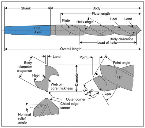
Innovative tool geometry design is more critical. Reducing drill point rake angle from conventional 30° to 15° increases cutting force but enhances edge strength, suppressing plastic flow. Adjusting helix angle from 40° to 35° maintains chip removal capability while reducing chip spiral curvature radius to promote breakage. A German tool manufacturer’s “dual-wave edge” technology creates periodic corrugations on cutting edges (0.8mm wavelength, 0.05mm amplitude), inducing mandatory bending strain that increases chip breakage probability to 92%.
Coating Technology for copper board drilling
In coating technology, multilayer composite coatings demonstrate unique advantages. The base layer uses 1μm-thick CrN to improve bonding strength, the intermediate layer is a 0.5μm MoS? solid lubricant layer, and the surface layer deposits 2μm diamond-like carbon (DLC) film. This structure reduces the friction coefficient from 0.6 to 0.15 and decreases adhesion by 80%. A Taiwanese PCB manufacturer using this coated drill for 6-ounce thick copper boards increased tool life from 1,200 to 4,500 holes while maintaining hole wall roughness Ra below 1.6μm.
New Opportunities from Material Modification
Material engineers are seeking breakthroughs in copper foil itself. Adding 0.3%-0.5% tellurium forms Cu-Te alloy, maintaining conductivity (≥85% IACS) while increasing tensile strength to 350MPa and controlling elongation at about 15%. This moderate plasticity reduction shortens chip fracture length by 40%. Another innovative approach develops anisotropic copper foil through rolling processes that align grains along the drilling direction, utilizing crystallographic texture effects to reduce transverse plasticity. Tests show this copper foil reduces chip entanglement by 65% when processing 0.3mm diameter holes.
Nanostructured Surface Treatment
Laser-textured microdimple arrays (20μm diameter, 5μm depth, 50μm spacing) on copper foil surfaces provide new solutions for adhesion challenges. These microstructures act as lubricant reservoirs, continuously releasing nano-MoS? particles. During drilling, these solid lubricants form transfer films at the tool-workpiece interface, reducing interfacial shear strength to 1/3 of pure copper systems. Japanese research data shows this method decreases drilling axial force by 28% and reduces adhesive wear by 90%.
Closed-Loop Control in Smart Manufacturing Systems
Under Industry 4.0 framework, thick copper board drilling is evolving toward digital closed-loop control. Integrated multi-physics sensors monitor spindle current (±0.1A sensitivity), acoustic emission signals (50-500kHz range), and infrared thermal imaging (0.1mm resolution). Deep learning algorithms establish cutting state recognition models that automatically adjust spindle torque output and trigger 0.8MPa high-pressure air knives for online chip removal when detecting entanglement frequencies (typically 120-180kHz).
Adaptive Control Systems
More advanced adaptive systems include intelligent drills developed by a U.S. equipment manufacturer that dynamically adjust processing strategies based on copper thickness: constant-force feed mode (120-150N cutting force) for 4-6oz copper, and step drilling (0.8× pilot hole + stepped feed) for >6oz copper. This strategy reduces tool load fluctuation by 40% and improves hole position accuracy to ±25μm.
Diversified Evolution of Future Technologies
Laser drilling breaks traditional machining limits. Picosecond lasers (10ps pulse width) with annular beam technology achieve <2° taper microholes in 100μm copper with <5μm heat-affected zones. Though currently 3-5× more expensive than mechanical drilling, it’s replacing conventional processes in high-density interconnects. Hybrid processing shows greater potential: laser-drilled 0.05mm pilot holes followed by micro-drill finishing improves efficiency by 70% and reduces tool wear by 90%.
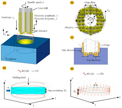
Ultrasonic-assisted Drilling Technology Enters Practical Application Stage
By integrating a 40kHz ultrasonic vibration device into the spindle, the drill bit generates high-frequency vibrations with 5μm axial amplitude. This vibration creates an “intermittent cutting” characteristic in the machining process, effectively releasing cutting stress periodically. When processing 8-ounce thick copper boards, the axial force is reduced by 35%, and chip thickness is decreased to 1/3 of conventional processes.
A more revolutionary breakthrough comes from cryogenic cutting technology. Using liquid nitrogen (-196°C) jets to locally freeze the cutting zone induces brittle transformation in copper, achieving brittle fracture mode. Preliminary tests show this method can completely eliminate chip entanglement, though it requires solutions for dimensional shrinkage compensation caused by low temperatures.
Conclusion
As PCB technology continues advancing toward high-power and high-density applications, solving thick copper board machining challenges has evolved beyond simple process improvements into a multidisciplinary innovation arena. From interfacial behavior research at the molecular dynamics level to intelligent control of macro manufacturing systems, each technological breakthrough redefines the limits of electronics manufacturing.
In the future, with the maturation of new material technologies like superconducting copper alloys and quantum dot lubricants, along with developments in atomic-scale manufacturing processes, thick copper board drilling will transition from the “problem-solving” stage to the “performance-design” stage, opening new frontiers for miniaturization and efficiency in electronic devices. This ongoing contest between copper and drill bits will ultimately propel the entire electronics manufacturing industry to higher dimensions of evolution.

